
News

Date2020-05-30/ Research Highlight
Following new research by Southern University of Science and Technology (SUSTech), the growth of all-inorganic metal halide perovskite single crystals on carrier transport layers could dramatically improve opportunities for emerging perovskite optoelectronic devices.
On April 22, Associate Professor Kai Wang (Electrical and Electronic Engineering) led his research group to publish a vital paper in the high-impact academic journal Advanced Science (IF = 15.804). Their paper was titled, “In Situ Growth of All-Inorganic Perovskite Single Crystal Arrays on Electron Transport Layer.”
Their paper focused on the essential problem of heterogeneous in-situ integration of the inorganic carrier transport layer and the all-inorganic metal halide perovskite single crystal in emerging optoelectronic devices.
Metal halide perovskites feature high deficit tolerance, adjustable energy bands, exciton binding energies, high quantum efficiency, and low cost of preparation. They are used in many different commercial applications and have been widely considered as encouraging optoelectronic materials.
Current research indicates that all-inorganic perovskite single crystals are usually grown on non-carrier transport material substrates or just in solution. They need to be further peeled off and transferred to the carrier transport layers, resulting in them sandwiched between transport layers in optoelectronic devices. It results in a highly complex preparation while also damaging the perovskite crystal layer. The deterioration of the interface between the perovskite active layer and the transport layer reduces the effectiveness of the carrier transport.
Therefore, growing the perovskite single crystals directly on the transport layer would solve most of the problems, but it is a challenging proposition to achieve.
The researchers prepared a cesium-lead-bromine (CsPbBr3) perovskite single-crystal array on an electron transport layer of cubic zinc oxide (c-ZnO) nanocrystals. The formation of the perovskite seed crystal layer on the surface of c-ZnO results in more stacked layers that continue to grow, achieving the in-situ growth of cubic CsPbBr3 perovskite single crystals on c-ZnO. The lattice that is formed provides a basis for expanding the choice of substrates (Figure 1 and 2)
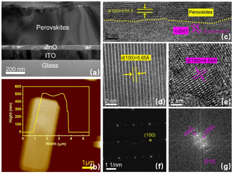
Figure 1. (a) SEM cross-sectional view of CsPbBr3 single crystal/c-ZnO interface; (b) AFM image of CsPbBr3 single crystal; (c) HRTEM image of CsPbBr3 single crystal/c-ZnO interface; (d) HRTEM image of CsPbBr3 single crystal; (e) HRTEM image of c-ZnO; (f) SAED image of CsPbBr3 single crystal; (g) FFT image of c-ZnO
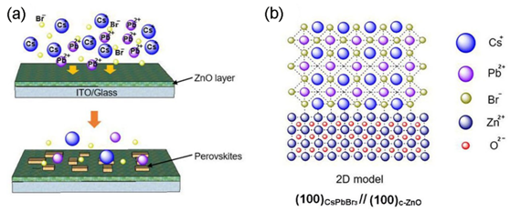
Figure 2. Schematic diagram of the heterogeneous in-situ growth mechanism of CsPbBr3 single crystal on c-ZnO.
In their analysis of the single crystals against perovskite nanocrystals, the researchers found that the array of single crystals provided strong scattered bright spots along the (100) scattering ring from the individual single crystal (Figure 3) while having a narrower energy state distribution. It resulted in a higher exciton diffusion rate and, therefore, better performance.
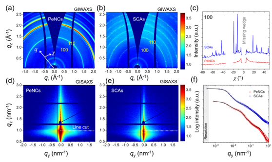
Figure 3. (a, b) Grazing-incidence wide-angle X-ray diffraction (GIWAXS) of CsPbBr3 nanocrystals and CsPbBr3 single crystal arrays; (c) (100) crystal plane orientation integration diagram; (d, e) Grazing-incidence small-angle X-ray diffraction (GISAXS) of CsPbBr3 nanocrystals and CsPbBr3 single crystal array; (f) Corresponding to the horizontal cut of the Yoneda peak position as indicated in (d) and (e) (structural analysis).
The results of this research confirm the possibility of in-situ growth of high-quality perovskite single crystals on the inorganic transport layer. Their integration forwards a significant step for the realization of better integration of perovskite single crystals and more other inorganic carrier transport layers and offers significant potential for the preparation of efficient and stable novel optoelectronic devices.
Research Assistant Xiaobing Tang and visiting student Wei Chen were the co-first authors of the paper. The co-correspondent authors of the paper were Associate Professor Kai Wang and Research Assistant Professor Dan Wu. Co-authors included Chair Professor Xiao Wei Sun (Electrical and Electronic Engineering), Professor Rui Chen (Electrical and Electronic Engineering), Associate Professor Mingyuan Huang (Physics), and Professor Peter Müller-Buschbaum (Technical University of Munich).
The authors received financial support from the National Natural Science Foundation of China, the National Key Research and Development Program, the Natural Science Foundation of Guangdong Province, the Guangdong University Key Laboratory for Advanced Quantum Dot Displays and Lighting, the High-Level University Fund of Guangdong Province, the Innovation Project of the Department of Education of Guangdong Province, the Shenzhen Peacock Team Prect, the Shenzhen Innovation Project, the Shenzhen Key Laboratory for Advanced Quantum Dot Displays and Lights, the Chinese Scholarship Council, and the German Research Foundation under Germany’s Excellence Strategy.
Link to the paper: https://onlinelibrary.wiley.com/doi/full/10.1002/advs.201902767