
News

Date2020-07-23/ Research Highlight
SUSTech researchers use black phosphorus for new direction in light-emitting devices
Mid-infrared (MIR) light-emitting devices play a crucial role in optical communications, thermal imaging, and material analysis applications. Researchers at Southern University of Science and Technology (SUSTech) have found a new use for black phosphorus in light-emitting devices.
On July 2, Assistant Professor Xiaolong Chen (Department of Electrical and Electronic Engineering) has led his research group to publish their research results in the high-impact academic journal, Light: Science & Applications (IF = 13.7). Their article was titled “Black phosphorus-based van der Waals heterostructures for mid-infrared light-emission applications.”
Black phosphorus (BP) is an emerging semiconductor of two-dimensional (2D) family. It has attracted significant attention due to its unique properties, such as in-plane anisotropy, high carrier mobility, and tunable bandgap. Moreover, its bandgap can be widely tuned, making BP a promising material for applications in MIR optoelectronics and photonics.
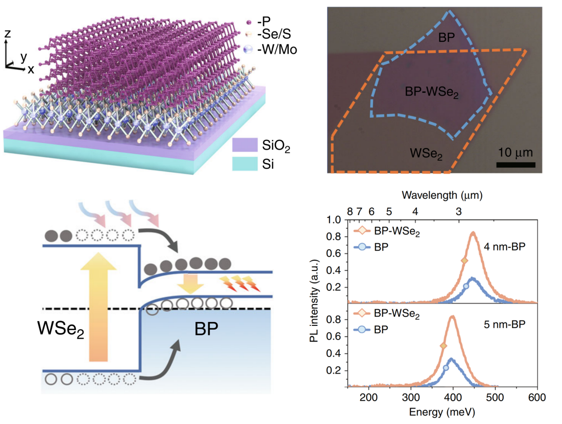
Figure 1: BP-WSe2 heterostructure for mid-infrared photoluminescence
The research group proposed a novel but straightforward van der Waals (vdW) heterostructure for MIR light-emission applications. They built the heterostructure from BP and transition-metal dichalcogenides (TMDC, such as WSe2 and MoS2). The first type of BP-WSe2 heterostructure formed a type-I band alignment. The optically excited excitons in the monolayer WSe2 were efficiently transported into the narrow-bandgap BP, thereby enhancing the MIR photoluminescence of thin-film BP (Figure 1).
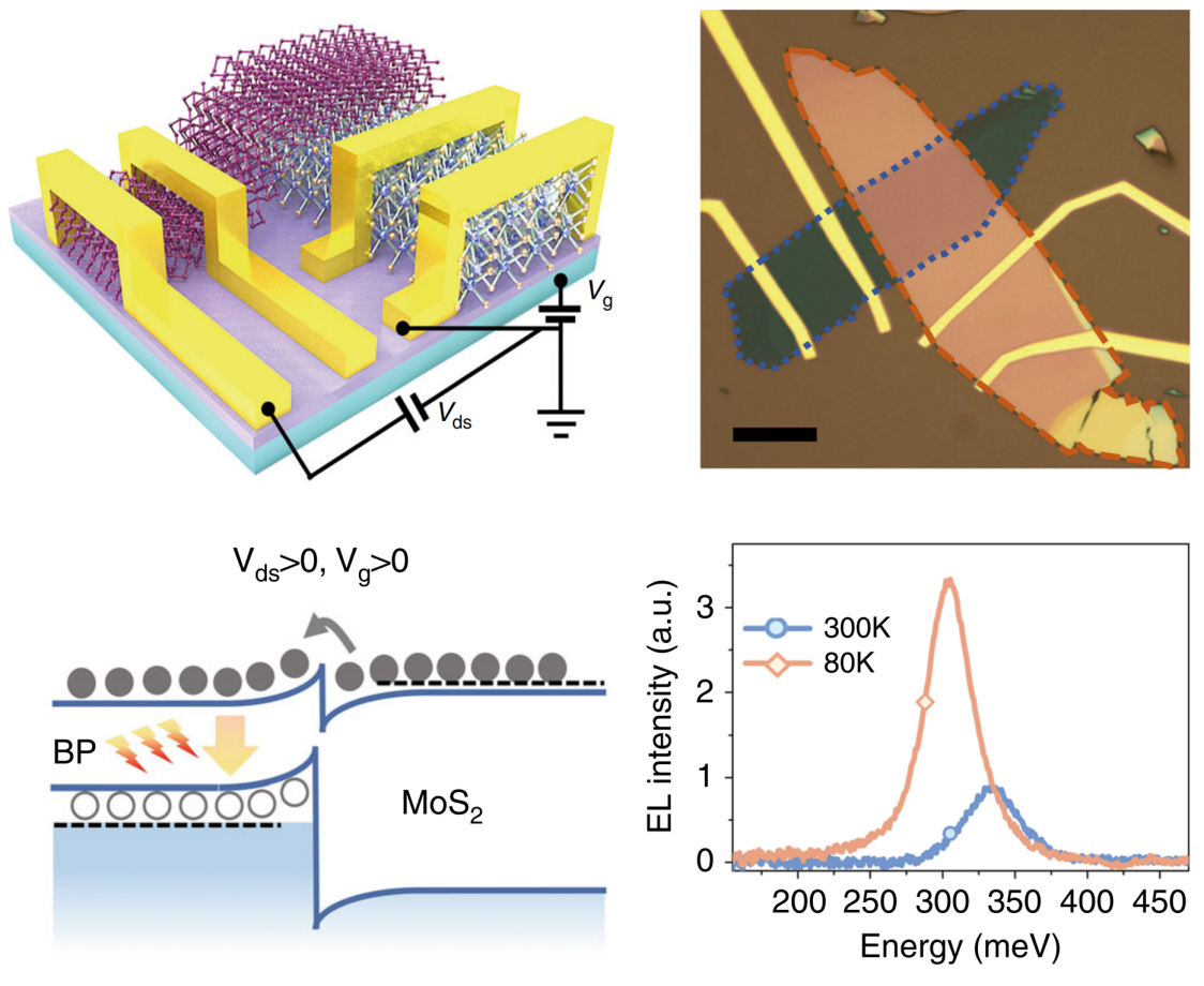
Figure 2: BP-MoS2 heterostructure for mid-infrared light-emitting diode
The second type of BP-MoS2 heterostructure formed a type-II band alignment. A natural PN junction was formed at the interface between p-type BP and n-type MoS2. When a positive voltage bias is applied between BP and MoS2 (Vds > 0), electrons in the MoS2 conduction band could cross the barrier and enter the BP conduction band. The majority of holes are also blocked at the BP interface, resulting from the large Schottky barrier of the valence band. An efficient MIR electroluminescence is achieved in the BP-MoS2 heterostructure (Figure 2).
The BP-TMDC vdW heterostructures show many merits, such as a simple fabrication process, high efficiency, and excellent compatibility with silicon technology. It, therefore, provides a promising platform for investigating silicon-2D hybrid optoelectronic systems.
SUSTech is the first corresponding unit for the paper. Assistant Professor Xiaolong Chen and Chair Professor Taihong Wang (Department of Electrical and Electronic Engineering, SUSTech) and Professor Lin Wang from Nanjing Tech University (Jiangsu National Synergetic Innovation Center for Advanced Materials) are the corresponding authors. Additional contributions came from Hunan Normal University, Shenzhen University, and Nanyang Technological University.
Assistant Professor Xiaolong Chen has also conducted a series of high impact research works on BP-based electronic and optoelectronic devices in recent one year. These research works have been published in high impact journals with SUSTech as the first corresponding unit, such as Nano Today (IF = 16.9), Advanced Optical Materials (IF = 8.3), and Advanced Electronic Materials (IF = 6.6). Besides, several high impact research works have been published with SUSTech as cooperating unit, including Science Advances (IF = 13.1) and Nano Letters (IF = 11.2).